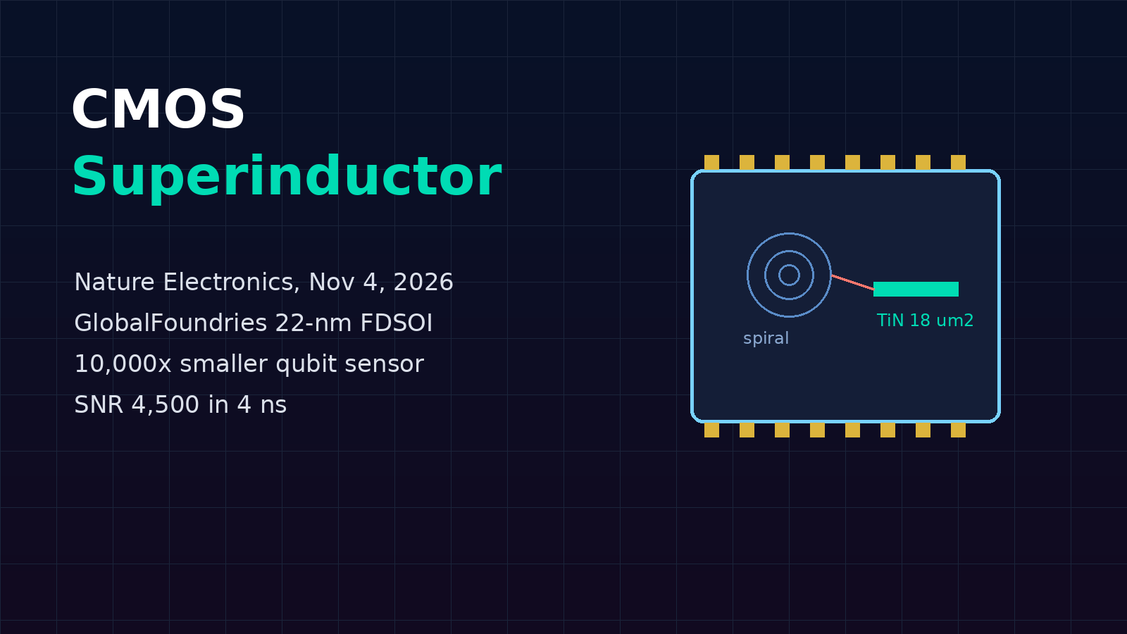
A team spanning Quantum Motion, CIC nanoGUNE, the London Centre for Nanotechnology, Imperial College London and the University of Cambridge reported in Nature Electronics on November 4, 2026 that it has built a true superinductor inside a commercial silicon chip, then used it to shrink a key spin-qubit readout sensor by more than 10,000 times. The device rides on titanium nitride (TiN) already present in GlobalFoundries’ 22-nm fully depleted silicon-on-insulator (FDSOI) process. Paired on the same die with a silicon quantum dot, it forms a radio-frequency single-electron transistor (rfSET) with an active footprint of just 18 μm² and a power signal-to-noise ratio of 4,500 in a 4 ns integration window. Here’s what was built, how the physics works and why it matters for anyone watching silicon spin qubits climb toward useful scale.
1. The Problem: Readout That Won’t Shrink
Silicon spin qubits are appealing because they look like ordinary transistors and can, in principle, be made on the same factory lines that already stamp out CPUs and phones. Reading them out is a different story. The workhorse charge sensor is the rfSET, and on a CMOS chip that sensor normally needs a large spiral inductor to reach a useful impedance. That spiral is visible by eye on a few-millimeter die, while the qubits it serves are nanometers across. As Quantum Motion staff engineer and lead author Tom Swift put it, “In quantum computing we talk a lot about scalability, but we focus mainly on the qubits themselves. In reality, we need to think about the scalability of the entire system.”
2. The Technology Behind It
A superinductor is not just a big coil. Its intrinsic impedance has to exceed the superconducting resistance quantum of about 6.45 kΩ. Conventional geometry-based spirals struggle to hit that target without eating the whole chip. The team instead leans on kinetic inductance: the inertia of charge carriers in a thin superconducting film. GlobalFoundries’ 22FDX stack already includes a TiN layer in the transistor gate stack. Below roughly 1 K, that film superconducts, delivering sheet kinetic inductances around 1 nH per square.
Key numbers from the paper and Quantum Motion’s summary:
- Footprint: active TiN strip area of 18 μm², more than four orders of magnitude smaller than a conventional on-chip spiral inductor
- Sensitivity: power SNR of 4,500 in 4 ns; extrapolated minimum time to SNR = 1 of 1 ± 0.3 ps, versus about 625 ps for the prior state of the art
- Process: commercial GlobalFoundries 22-nm FDSOI, no bespoke superconducting fab flow
- Nonlinearity: at higher drive power the TiN inductance itself becomes nonlinear, boosting the readout signal beyond ordinary amplitude sensing
- Transition temperatures: reported variants around 0.75 K and 1.1 K, so this is deep-cryogenic hardware, not a room-temperature RF part
VP of Quantum Engineering at Quantum Motion and nanoGUNE professor M. Fernando González-Zalba said the native CMOS superinductors “meet all the requirements for spin qubit readout” with a compact, low-power, highly sensitive on-chip footprint.
3. Why It Matters for Scalable Quantum Hardware
Every serious spin-qubit roadmap eventually collides with the same question: can the control and readout electronics shrink to something close to the qubit pitch? A sensor that is 10,000 times smaller than today’s spiral-based designs is a concrete step toward packing many more qubits onto a single CMOS die without drowning them in inductors. Because the work uses a film the foundry already deposits, it also strengthens the argument that useful quantum hardware can ride industrial process nodes instead of one-off research fabs.
The authors also flag applications beyond spin qubits, including parametric circuits, kinetic-inductance detectors, and one- and two-dimensional resonator arrays for quantum simulation and cryoelectronics. Those remain forward-looking; the demonstrated win is integrated charge sensing.
4. Limits Worth Keeping Straight
This is still laboratory hardware. Operation sits well below 1 K, internal resonator quality factors in the reported variants are modest (around 50), and the picosecond figure is an extrapolated sensitivity metric rather than a demonstrated readout clock. Parasitic capacitance estimates lean on foundry models, and wafer-level yield statistics are not yet the story. Think of it as a proof that the industrial CMOS toolkit can host the exotic circuit element quantum engineers have been building by hand.
Looking Ahead
Quantum Motion says the next step is to wire the rfSET to arrays of silicon spin qubits and show high-fidelity readout well below the microsecond mark. If that lands, the bottleneck shifts from “can we sense the qubit?” toward “can we route, multiplex and cool a million of them?”—which is exactly the systems problem Swift called out.
For IT pros watching the quantum hype cycle, the practical takeaway is quieter but important: credible progress is showing up in Nature Electronics as foundry-compatible building blocks, not just bigger qubit counts on custom chips. Silicon spin qubits still have a long road to fault-tolerant machines, but shrinking the readout to the scale of the qubit is one of the unglamorous pieces that has to move before the glossy roadmaps mean anything on a rack.
Sources:
- Nature Electronics (Swift et al., “A nonlinear superinductor in a deep-submicrometre integrated circuit”), November 4, 2026
- Quantum Motion, November 4, 2026
- CIC nanoGUNE, November 4, 2026
- Passive Components (technical summary), November 5, 2026