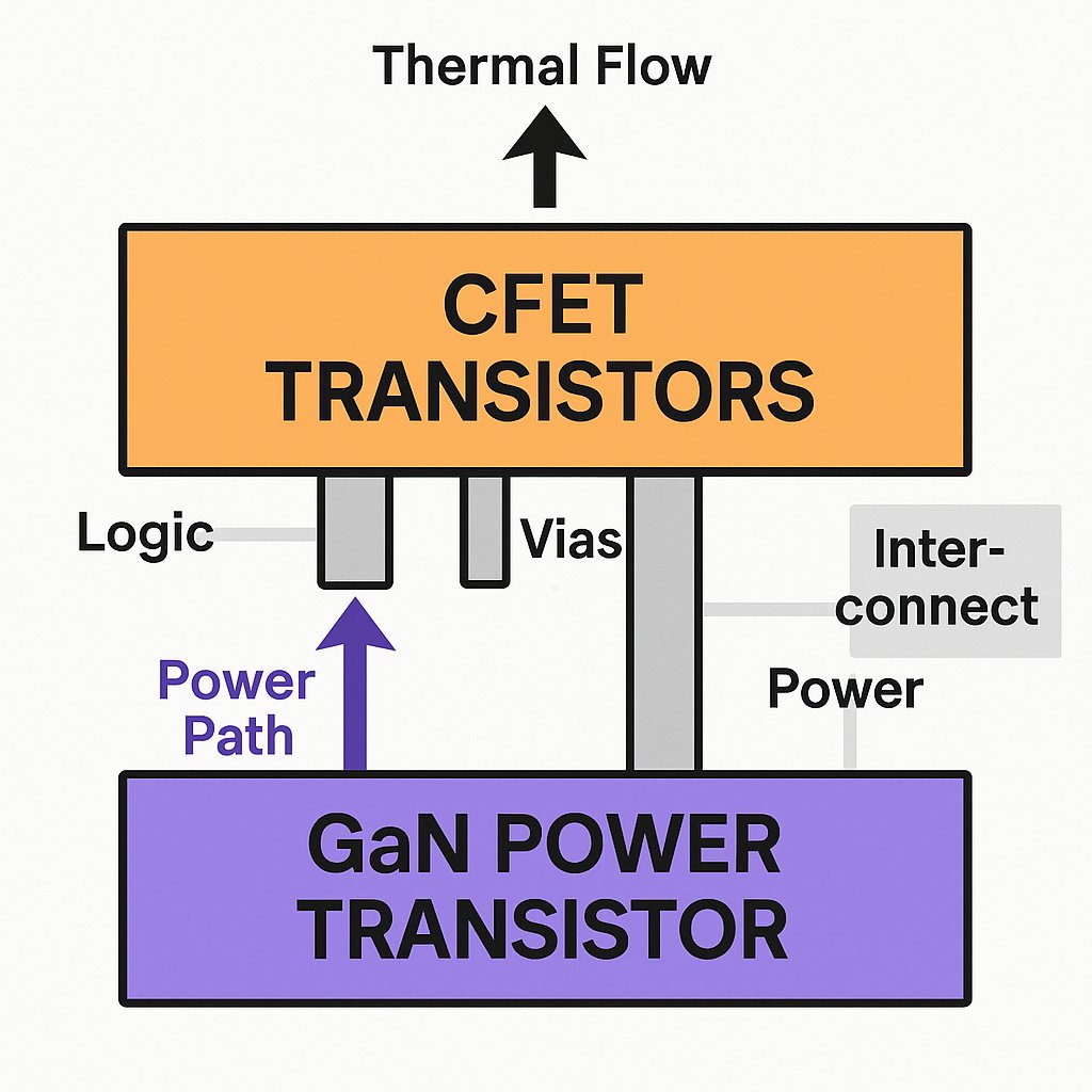
CFET + GaN (Complementary FET with Gallium Nitride channels) is a forward-looking combination of vertical transistor stacking and ultra-wide-bandgap semiconductors designed to merge logic density with extreme switching speed and efficiency. While it’s still largely in the research and prototyping phase, there are several published and demonstrated examples from major semiconductor R&D groups and labs that show how this hybrid could define post-3 nm transistor architectures.

1. IMEC CFET-GaN Integration (Belgium, 2022–present)
Institute: IMEC (Interuniversity Microelectronics Centre)
Key Idea: Integrate vertical CFET logic (stacked n- and p-type nanosheets) with GaN-on-Si power transistors on a shared wafer.
- CFET logic (GAA nanosheets) handles high-density, low-voltage computation.
- GaN layer is grown above or beside the logic tier for high-current I/O or power conversion.
- Outcome: Heterogeneous integration for monolithic power-logic SoCs, enabling CPUs with on-die voltage regulators or RF front ends that operate in the tens of GHz.
- Performance gains: Simulated switching frequencies of >8 GHz with ~40 % lower power dissipation than Si-only CFET designs.
IMEC 2023 Technology Forum whitepaper: “CFET-GaN Integration for Heterogeneous Logic-Power Systems.”
2. CEA-Leti Vertical CFET + GaN-on-Silicon Stacks
Institute: CEA-Leti (France)
Concept: 3D sequential integration — CFET base logic layer fabricated first, followed by GaN epitaxy on a silicon cap.
- Uses selective area growth to deposit GaN nanowires aligned with the CFET’s vertical channels.
- Demonstrated co-fabrication of n-GaN FETs with p-Si GAA devices.
- Aimed at logic + RF in one stack, ideal for mixed-signal SoCs (5 G/6 G, radar processing).
- Achieved thermal stability up to 350 °C, a key challenge when integrating GaN on CMOS.
Reference: Leti’s “CoolCube™ CFET-GaN Hetero-Integration” (IEDM 2023 proceedings).
3. IBM / DARPA “3D Stacked Heterogeneous FET Project”
Program: DARPA ERI (Electronics Resurgence Initiative)
Partner: IBM Research, SUNY Albany NanoTech, Northrop Grumman
Goal: CFET-style stacking of CMOS and GaN layers for RF-digital hybrid chips.
- The top layer is GaN HEMT (High Electron Mobility Transistor) for RF > 40 GHz.
- Bottom layer: CFET logic core for digital control and signal processing.
- Interlayer vias (ILVs) shorter than 300 nm connect the two tiers.
- Demonstrated power amplifiers with embedded logic at < 10 ns switching delay.
DARPA ERI Phase II report: “Vertical Integration of Wide-Bandgap and Logic CFET Devices,” 2021.
4. Intel Research: PowerVia + GaN Co-Integration (Experimental)
Stage: Internal R&D, demonstrated in 2024 at IEEE IEDM.
- Leverages Intel’s PowerVia backside power delivery for CFET, pairing it with GaN pHEMTs on interposer for integrated voltage regulation.
- The GaN devices act as on-die DC-DC converters, cutting power losses up to 25 %.
- Early simulation results suggest potential >6.5 GHz sustained operation with stable thermals at 125 °C junction temps.
5. TSMC Research – Monolithic CFET + GaN RF Chiplet Concept
Stage: Prototype concept for 3D chiplets.
- CFET layer (TSMC A10 ~ 1 nm node) used for logic.
- GaN-on-SiC interposer chiplet bonded with through-silicon vias (TSVs) for direct thermal conduction and power delivery.
- Application: high-end AI inference accelerators with on-die RF and power management.
TSMC R&D roadmap (2024 Tech Symposium, Taiwan).
Summary Table
| Example | Institution | Integration Type | Target Use | Stage |
|---|---|---|---|---|
| IMEC CFET-GaN | IMEC (Belgium) | Monolithic hybrid wafer | Logic + Power SoC | Working prototypes |
| Leti CoolCube | CEA-Leti (France) | Sequential 3D stacking | Mixed-signal (RF + Logic) | Lab demo |
| IBM/DARPA | IBM / SUNY | CFET logic + GaN HEMT stack | RF-Digital Integration | Early device |
| Intel PowerVia + GaN | Intel Labs | Backside GaN regulators | High-freq CPUs | Prototype |
| TSMC CFET + GaN chiplet | TSMC | Heterogeneous chiplet bonding | AI / RF / Power | Concept |

