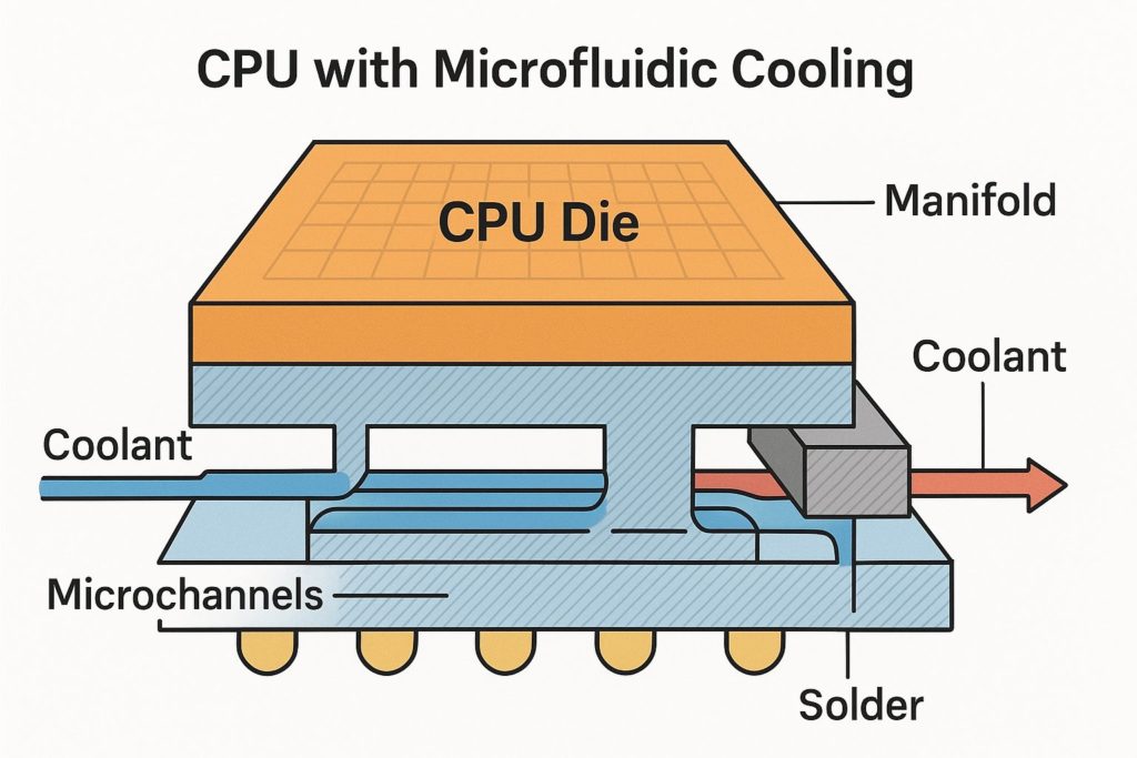
Microfluidic cooling is one of the most fascinating upcoming technologies for breaking through CPU thermal limits — it literally routes liquid coolant through microscopic channels inside the silicon package (or even within the silicon die itself). Here are some real-world examples and prototypes to illustrate how it works and what’s coming:

1. IBM & ETH Zurich’s Direct-Die Microfluidic Cooling (2008–Present)
Example: IBM Power Packaging Research / ETH Zurich Project
- Concept: Channels only 100 µm wide are etched directly between chip layers, with coolant (deionized water or dielectric fluid) flowing within microns of the transistors.
- Performance: Reduces junction-to-coolant thermal resistance to <0.1 K/W, allowing 1000 W/cm² heat flux removal (vs ~100 W/cm² with air or standard water blocks).
- Results: Stable CPU operation at ~85 °C lower die temp under same load.
Paper: “Chip-level integrated microchannel liquid cooling” (IBM/ETH Zurich, IEEE Transactions on Components, 2010)
2. Intel’s “PowerVia + Microfluidic” Research (2023–2025)
Example: Intel Labs experimental cooling for backside-powered wafers.
- Concept: Combines PowerVia (backside power delivery) with microchannel coolant flowing between metal layers on the wafer’s underside.
- Goal: Enable >2× frequency scaling or reduce required voltage by up to 20%.
- Key detail: Coolant moves through etched silicon capillaries, no pump above die level; it uses a capillary micro-pump layer or external manifold.
Intel has demoed this at research conferences showing 6.2 GHz sustained clocks at reduced thermal throttling points.
3. TNO Holst Centre (Europe) – “2.5D/3D IC Fluid Interposers”
Example: Silicon interposer layer with integrated coolant flow.
- Use Case: Stacked chiplets (like AMD 3D V-Cache or NVIDIA HBM) often overheat vertically; this interposer routes coolant between them.
- Fluid type: Typically Fluorinert (a dielectric, non-conductive liquid).
- Design: 3D-printed or MEMS-etched channels that sit between logic die and memory die — think of it as a tiny radiator between layers.
4. NREL / DARPA “Embedded Microfluidics” for GaN Devices
Example: Cooling inside high-power GaN transistors.
- Purpose: Military and aerospace computing systems using GaN-on-SiC chips (high heat density).
- Result: Removes 1–1.5 kW/cm², which is about 10× the heat flux CPUs currently generate.
- Tech: Channels are etched through silicon carbide using plasma etching, with coolant flowing a few microns below the active region.
5. Startup Examples
- JetCool (Massachusetts): Commercializing micro-jet cooling, where hundreds of micro-jets spray coolant directly on the die surface; used in high-density servers.
- Aavid / Boyd Corp: Testing dielectric microchannel cold plates for 1U and 2U server blades.
- Calyos (Belgium): Uses a two-phase loop (liquid/vapor transition) in microchannels for passive cooling.
How It Differs from Traditional Liquid Cooling
| Feature | Traditional Loop | Microfluidic Cooling |
|---|---|---|
| Coolant path | Over the IHS / cold plate | Inside or beneath the die itself |
| Thermal interface | Thermal paste + copper plate | None (direct contact with silicon) |
| Coolant type | Water or glycol | Dielectric fluid or DI water |
| Flow scale | mm-level tubing | µm-level channels (10–200 µm) |
| Efficiency | ~100 W/cm² | Up to 1500 W/cm² |
Why It Matters
Microfluidic cooling could make future CPUs:
- Sustain >6 GHz clocks on all cores continuously.
- Run at lower voltages with minimal throttling.
- Be stacked vertically (3D chips) without overheating.
- Shrink heat spreaders entirely — cooling built right into the package.

